Intel announced Edison, a miniature computer based on the Quark SoC technology housed on the form factor of an SD card. Intel Edison built on 22nm transistor technology, runs Linux and has built-in Wi-Fi and Bluetooth modules.
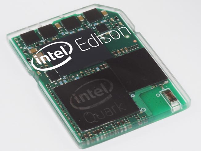
Intel announced Edison, a miniature computer based on the Quark SoC technology housed on the form factor of an SD card. Intel Edison built on 22nm transistor technology, runs Linux and has built-in Wi-Fi and Bluetooth modules.
Lava mobiles Xolo X900 launching the Xolo X900 smartphone which also becomes the first Intel powered smartphone in the world on 23rd April 2012.
Intel Labs demonstrated an experimental, 48-core Intel processor, This chip is 10 to 20 times the processing power of today’s most popular Intel Core-branded processors. It also includes a high-speed on-chip network along with new power management techniques allow all 48 cores to operate extremely energy efficiently at as low as 25 watts, or at 125 watts at maximum performance.
As We know Intel already Demonstrated the working 32nm processor. Paul Otellini, Intel’s CEO has revealed that Intel already shipped its new 32nm Westmere samples to its partners. These processors are expected by this end of year.
10th, Feb 2009 San Francisco, Intel corp, World’s largest semiconductor company demonstrated the first working 32nm processor. Intel Corporation discussed new milestones for 32nm manufacturing and progress toward future products. Working intel 32nm processor Summary of the Roadmap at the briefing in San Francisco: First-ever demonstration of a working 32nm-based microprocessor: Intel is demonstrating the first 32nm working microprocessor in…
Nehalem, Intel new architecture is not yet officially launched,? But we got information about it’s successors, on which? intel is working on. The new CPU therefore follow the pattern of development “Tick-Tock”, i.e; a new architecture every two years (Tock), followed by a die shrink (Tick). In exclusivity, here are the code names of future generations of processors, and until 2012…
Intel ® recently released the mobile platform Centrio2 and heading towards nehalem based laptop platform named as “Calpella”. Calpella to support WiMAX in addition to b/g/n WiFi. As with other Nehalem generation products, Capella will also rearrange the components like abandon the current northbridge and memory control is moving into the CPU package. A single integrated chipset codenamed Ibex Peak‑M…