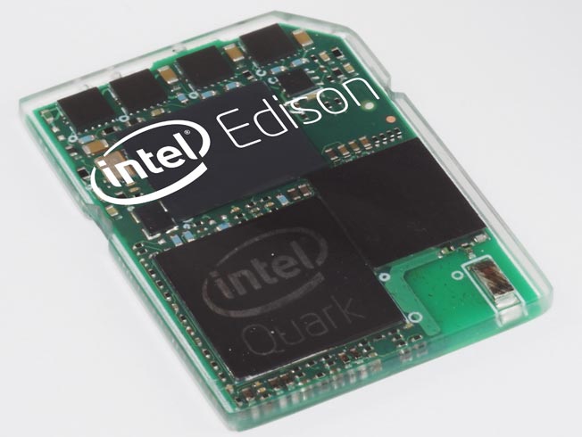
Nehalem, Intel new architecture is not yet officially launched,? But we got information about it’s successors, on which? intel is working on. The new CPU therefore follow the pattern of development “Tick-Tock”, i.e; a new architecture every two years (Tock), followed by a die shrink (Tick). In exclusivity, here are the code names of future generations of processors, and until 2012
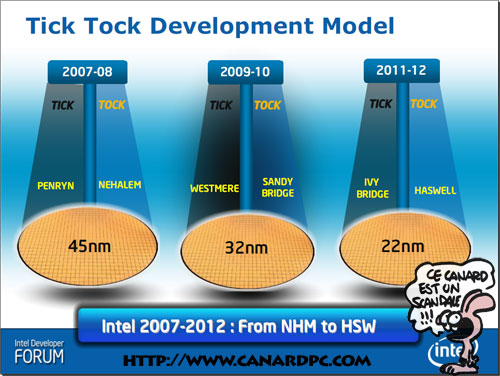
- West Mere (Tick, 2009, 32 nm)
- Sandy Bridge (Tock, 2010, 32 nm)
- IVY Bridge (Tick, 2011, 22 nm)
- Haswell (Tock, 2012, 22 nm)
Currently Penryn (Tick, 2008, 45nm) are available in market which are engraved in 45nm die. At the end of the 2008 the new generation Nehalem(Tock, 2008, 45nm) engraved in 45nm die. Then the Westmere(Tick, 2009, 32nm) Nehlam architecture engraved in 32nm die. Then comes Sandybridge(Tock, 2010, 32nm) engraved in 32nm die. And it goes to Ivy Bridge(Tick, 2011, 22nm) then to Haswell(Tock,2012,22nm) engraved in 22nm die.
First We talk about Nehalem, Which is successor of core2 architecture mainly comes with more number of cores(upto 8), cache, Integrated memory controller. Nehalem will have 32 KB L1 cache Data, 256 KB L2 cache with very low latency by heart and a L3 cache of varying size (up to 8 MB on the Desktop versions). Nehalem will also have the Hyperthreading, which allows the execution threads 2 by heart. The effectiveness of this technology on this type of architecture at short pipeline remains questionable.
Sandy Bridge, the next Intel architecture. So far about this to the fact that they are manufactured in 32 nm would and would likely 2010. It comes with AVX, was not necessarily directly with Sandy Bridge in connection. Now, however: Sandy Bridge is the first Intel CPU, the AVX, the SSE successor. Supposedly AVX similar take as SSE 1999 to the Pentium processors. The following lists the grossest film improvements.
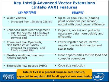
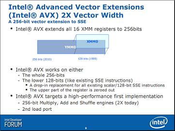
- The extension of the current SSE registers 128 to 256 bits, while remaining compatible with 128-bit SSE instructions.
- The rearrangement advanced data: a single operation can simultaneously handle 8 data bits 32
- The possibility to use three or four operands
For Sandybridge, each core will be given on a 512 KiB large L2 cache, while a 16 MB large L3 cache accessible to all cores.
Haswell, Planned for 2012 or earlier, the family Haswell successor architecture of Sandy Bridge. engraved to 22 nm, they should include 8‑core default, a whole new architecture caches, “revolutionary” energy saving and the possibility of board coprocessors vector processing in a single package. New instruction set, FMA (Fused Multiply-Add), which allows simultaneous operation of multiplication and addition via the same instruction, should be implemented.